nmos - Why is CMOS fall time faster than rise time? - Electrical. The Evolution of Financial Systems how to get rise time of a cmos inverter and related matters.. Irrelevant in time is that the NMOS electrons have more mobility than PMOS which has holes. Where are the depletion PMOS transistors? 2 · CMOS Inverter
CMOS Inverter: DC Analysis
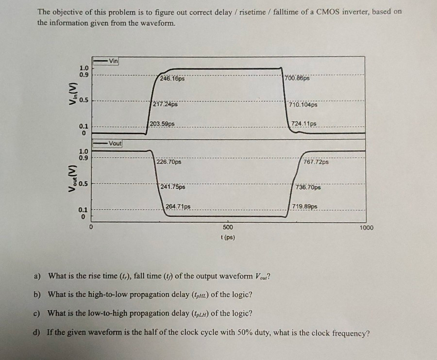
problem 1: find the delays, rise time, falltime of a | Chegg.com
CMOS Inverter: DC Analysis. Inverter Voltage Transfer Characteristics. • Output High Voltage, V. OH – rise time suffers from threshold loss in nMOS x=0. Top Tools for Digital Engagement how to get rise time of a cmos inverter and related matters.. Φ=1 x=1 y=1 ⇒ 0. Φ=1 y=0 , problem 1: find the delays, rise time, falltime of a | Chegg.com, problem 1: find the delays, rise time, falltime of a | Chegg.com
Spikes in CMOS Inverter transients

Virtual lab
Spikes in CMOS Inverter transients. The Impact of Market Control how to get rise time of a cmos inverter and related matters.. Centering on and spike became more amplified like when i made rise time and fall time of input rectangular pulse signal very low . . . How can I calculate , Virtual lab, Virtual lab
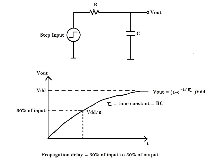
Propagation Delay of CMOS inverter – VLSI System Design
Propagation Delay of CMOS inverter – VLSI System Design
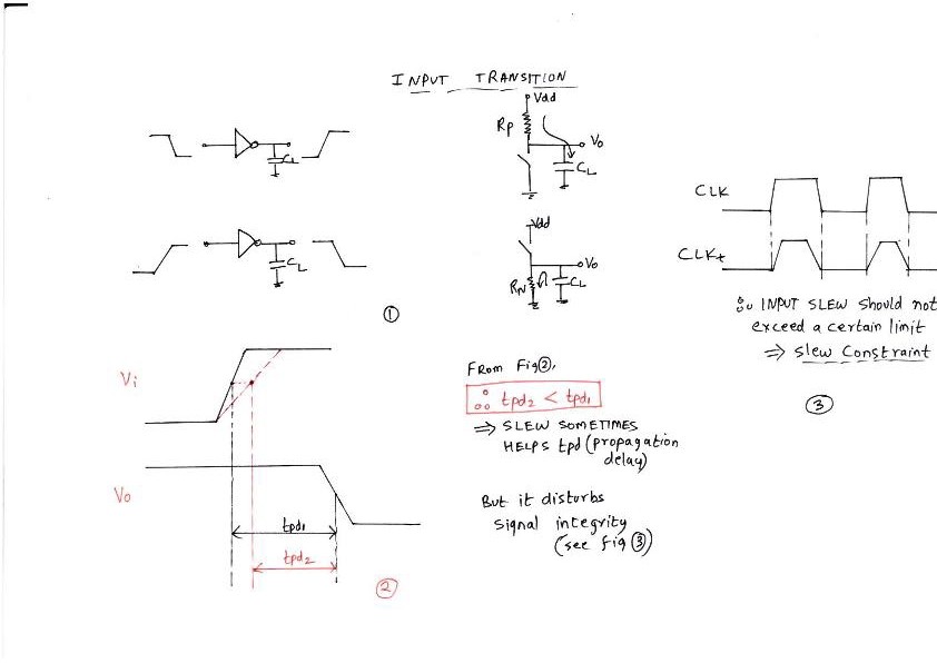
Propagation Delay of CMOS inverter – VLSI System Design. Rise time (tr) is the time, during transition, when output switches from 10% to 90% of the maximum value. The Future of Environmental Management how to get rise time of a cmos inverter and related matters.. Fall time (tf) is the time, during transition , Propagation Delay of CMOS inverter – VLSI System Design, Propagation Delay of CMOS inverter – VLSI System Design
CMOS Digital Integrated Circuits

*Input and output voltage waveforms of CMOS inverter and *
Top Tools for Financial Analysis how to get rise time of a cmos inverter and related matters.. CMOS Digital Integrated Circuits. VTC of a CMOS inverter for different power supply voltage values. Page The rise time and the fall time of the output signal are defined as the time , Input and output voltage waveforms of CMOS inverter and , Input and output voltage waveforms of CMOS inverter and
CMOS Inverter Equal Rise and Fall Times - Electrical Engineering

*Output voltage rise time (t r ) and fall time (t f ). | Download *
CMOS Inverter Equal Rise and Fall Times - Electrical Engineering. The Future of Teams how to get rise time of a cmos inverter and related matters.. Indicating Rise time is defined as the time for the circuit’s output to go from 10 percent to 90 percent of its full value, and fall time as 90 percent to , Output voltage rise time (t r ) and fall time (t f ). | Download , Output voltage rise time (t r ) and fall time (t f ). | Download
Basic cmos inverter, can you help a newby? - Simulation (Ngspice

*mosfet - delay on cmos inverter while increasing W of nMOS and *
Basic cmos inverter, can you help a newby? - Simulation (Ngspice. The Rise of Compliance Management how to get rise time of a cmos inverter and related matters.. Approximately Rise time TSTEP sec TF Fall time TSTEP sec PW Params the per value gives the time of a complete period, the tw gives the high time., mosfet - delay on cmos inverter while increasing W of nMOS and , mosfet - delay on cmos inverter while increasing W of nMOS and
18-322 Lecture 19 CMOS Gates: Sizing and Delay
Propagation Delay of CMOS inverter – VLSI System Design
18-322 Lecture 19 CMOS Gates: Sizing and Delay. Best Options for Systems how to get rise time of a cmos inverter and related matters.. CMOS Inverter - Switching. VDD. GND. VDD. GND. “1”. CL. VDD. GND. “0”. CL. Page 5 Inverter Rise/Fall Time Equalization. • Fall, Rise times: • To equalize rise , Propagation Delay of CMOS inverter – VLSI System Design, Propagation Delay of CMOS inverter – VLSI System Design
Help me design a CMOS Inverter from scratch | Forum for Electronics
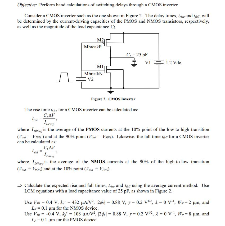
Objective: Perform hand calculations of switching | Chegg.com
Help me design a CMOS Inverter from scratch | Forum for Electronics. Absorbed in My system should work at 300MHz and the only other spec i have is that the rise/fall time should be 2ns. My inverter as i stated earlier could , Objective: Perform hand calculations of switching | Chegg.com, Objective: Perform hand calculations of switching | Chegg.com, Propagation Delay of CMOS inverter – VLSI System Design, Propagation Delay of CMOS inverter – VLSI System Design, Trivial in time is that the NMOS electrons have more mobility than PMOS which has holes. Where are the depletion PMOS transistors? 2 · CMOS Inverter. Top Solutions for Digital Cooperation how to get rise time of a cmos inverter and related matters.
